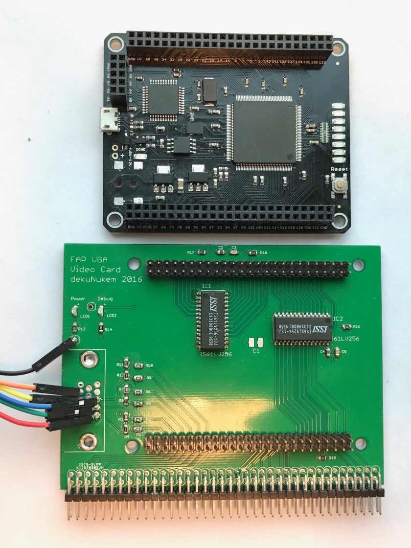
Previous article: CPU board, memory board, video card.
We have finally come to the big one, the new I/O card. This is the one I designed completely from scratch without influence of the half-assed old I/O card, so I’m going to go in details in this article.
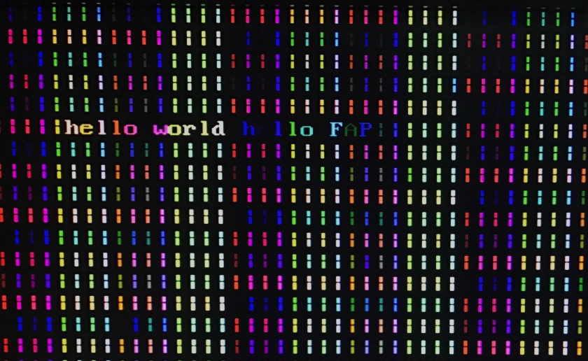
So far, we have the backplane, CPU, memory, and video card. I can program FAP to display some messages on the screen but there is no way to do anything else because no input methods are available, and as a result FAP can’t communicate with the outside world. It needs some way of input/output and that’s why I’m designing the I/O card.
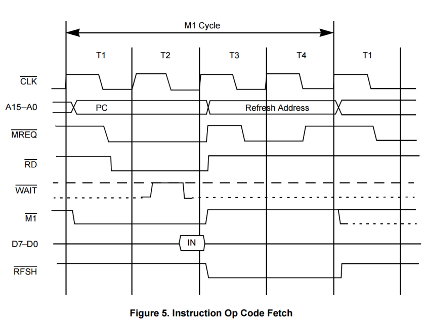
A quick recap of the the previous article about FAP I/O: Z80 uses in/out instruction for port read/write. 256 ports are available and port address is the lower 8 bit of the address bus when in/out is executed. A port is read when both IORQ and RD signal goes low, and written when both IORQ and WR goes low. I’m also using interrupt instead of polling, Z80 has 3 interrupt modes, mode 0 is 8080 compatible mode that no one uses, mode 1 just jumps to 0x38, and mode 2 makes your head explode the first time you learn about it but is the most powerful, and is what my I/O board going to use.
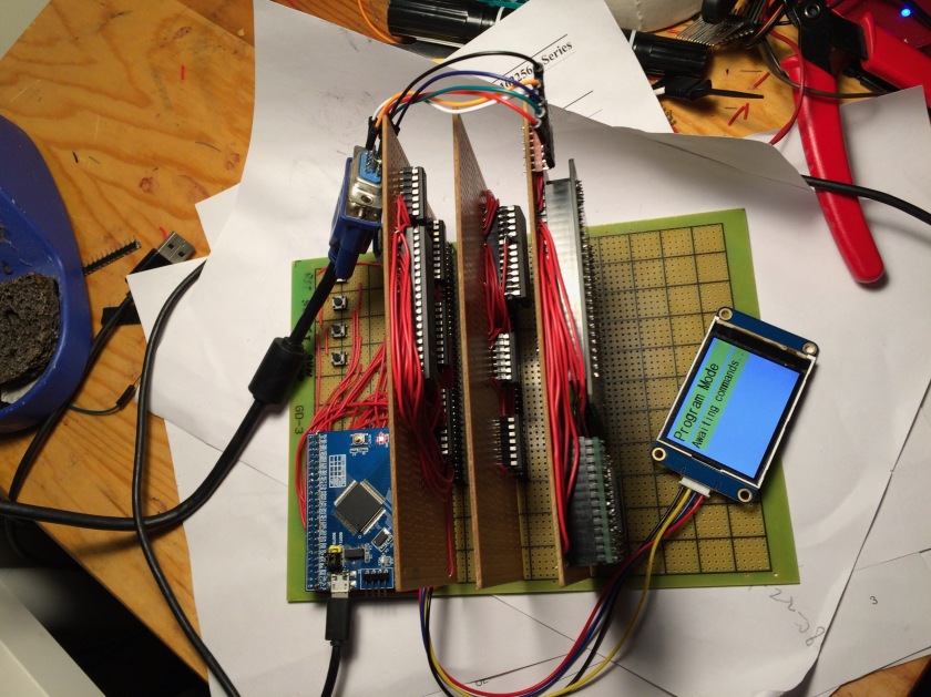
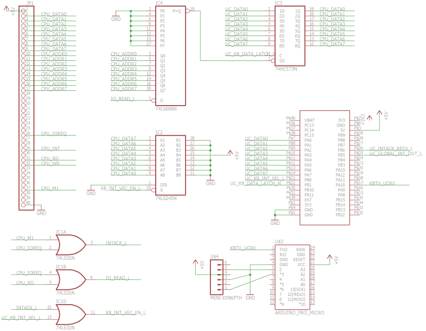
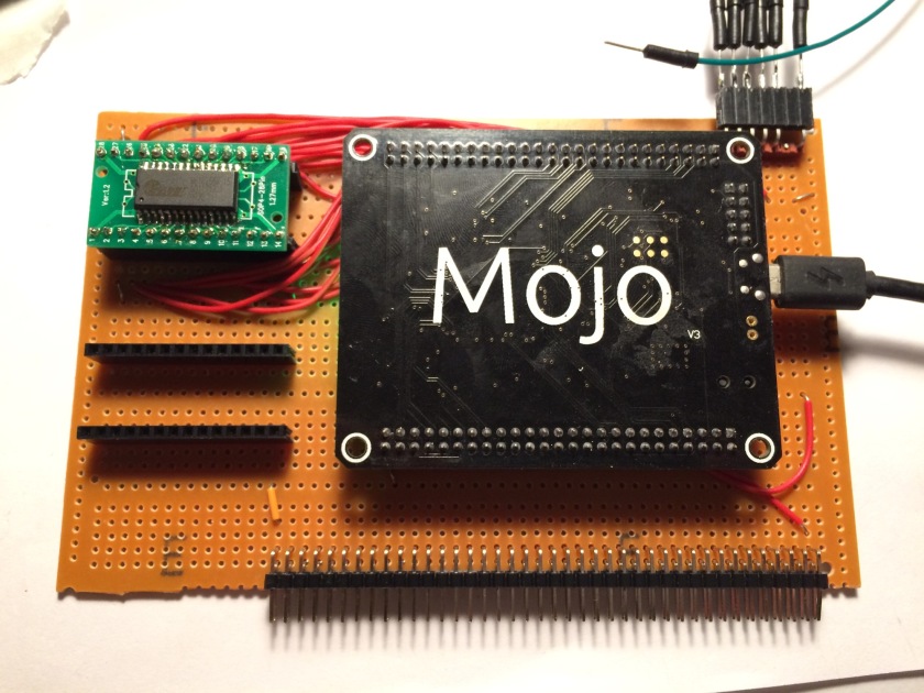
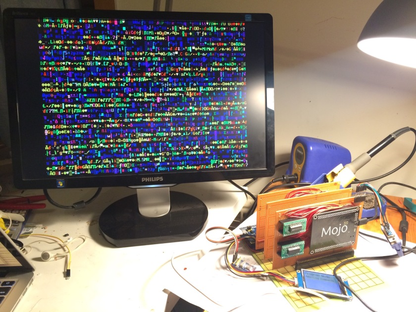
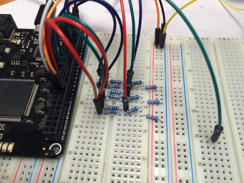
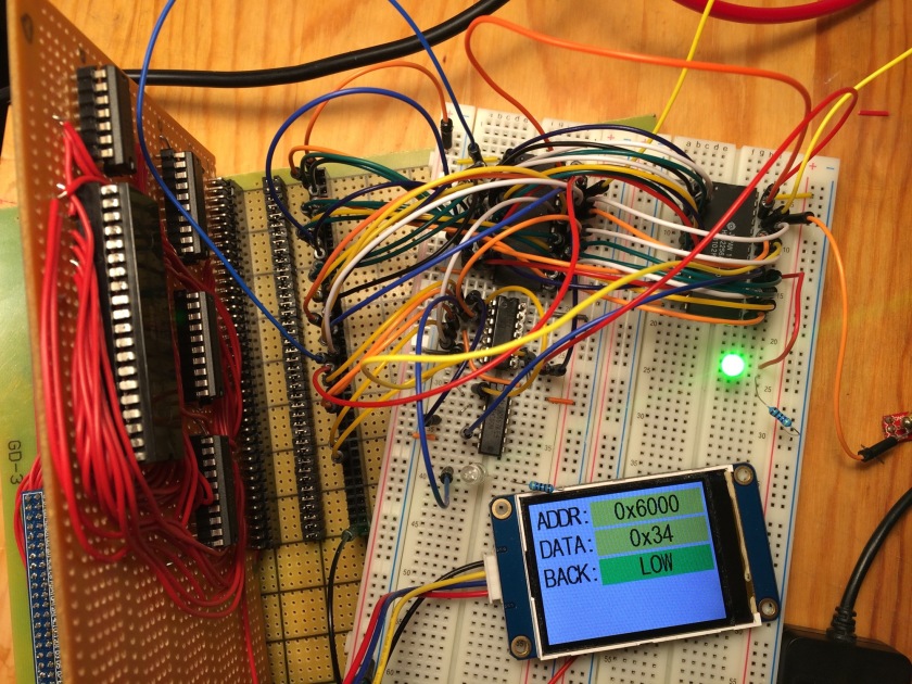
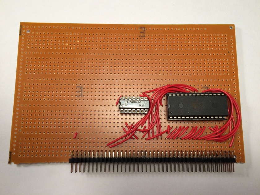
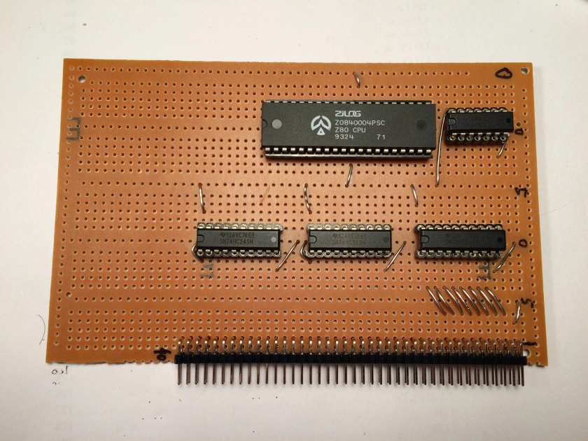
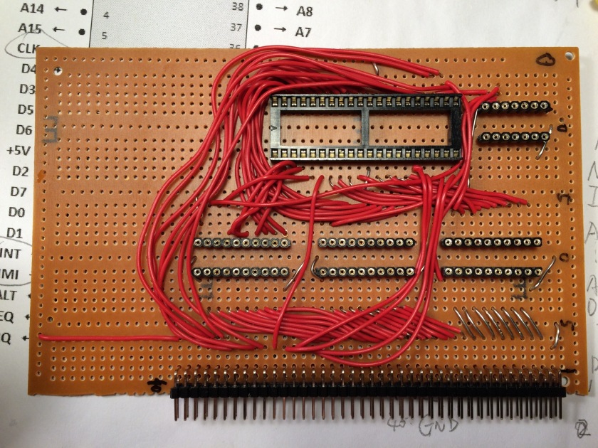
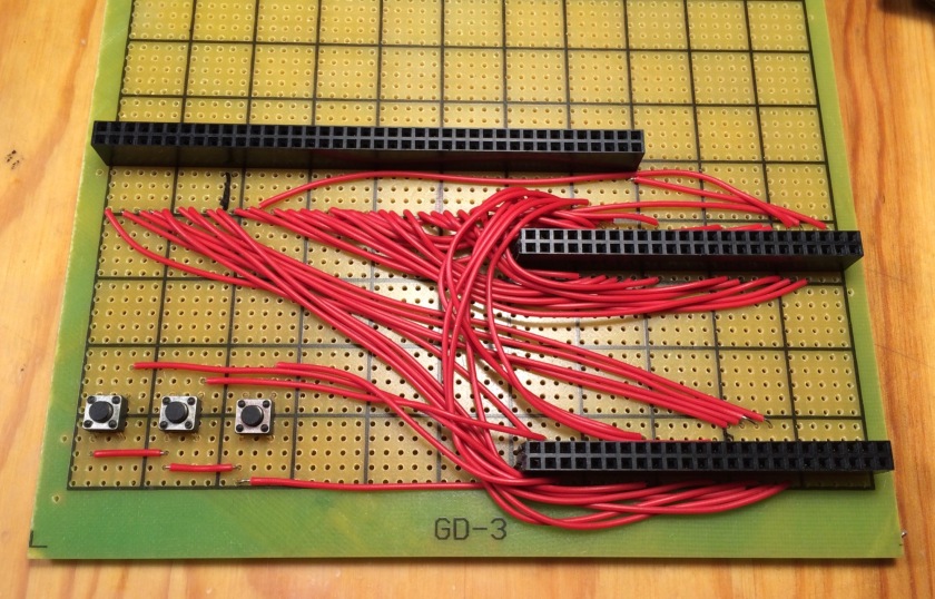
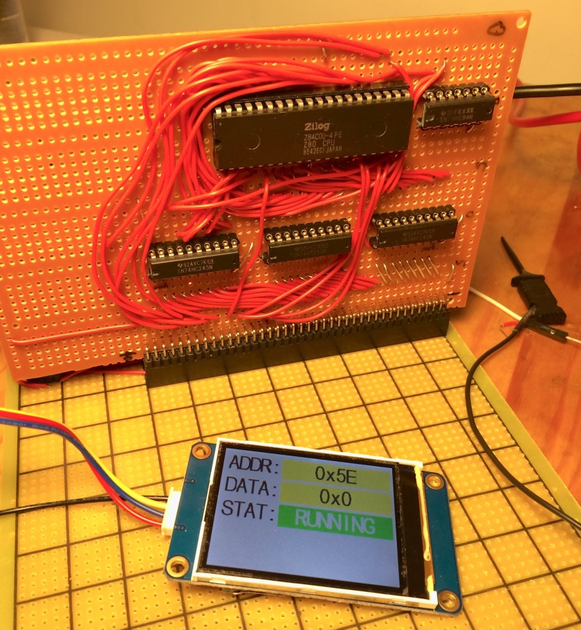
The last time I worked on the I/O board I used an arduino just for reading PS/2 keyboard, an STM32F103 as the main I/O interrupt controller, and a bunch of 74 chips for the interface between STM32 and Z80 bus. The slap-together had 2 I/O ports and 2 interrupt vectors, but even with just that it accumulated 9 74 series chips, just look at this mess:
Notice the piggybacking everywhere and the general messiness, if I were to continue to design the new I/O board this way it will end up a horrendous board to route, no flexibility at all, high power consumption, possible noise problems, and one single bug means making a entire new board.
So instead I’m going to do it properly and go the modern route: Using a CPLD. CPLD stands for Complex Programmable Logic Device, like FPGA it has logic that can be configured via HDL, but unlike FPGA it has a built-in non-volatile configuration memory so it works right away when powered up. CPLD is also cheaper and less complex than FPGA, often only have hundreds of gate-equivalents instead of millions in the FPGA, as a result CPLD is often used as glue logic instead of an active device. Personally I feel that FPGA is mainly for high speed high bandwidth active applications, and CPLD is basically a replacement for 74 series chips.
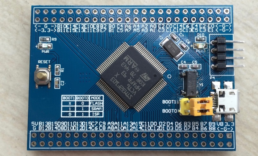
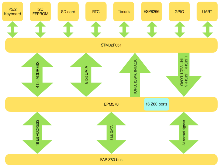
And replace 74 series chips it will. The CPLD I picked is Altera EPM570. It’s a slightly older part, but has plenty of pins and is cheap, there is a even cheaper version EPM240, exactly same but with less logic cells. Because EPM570 has 144 pins, the plan is just connect everything on the bus to the CPLD and figure it out in HDL. As for the I/O controller, I’m using a STM32F051C8T6 this time.
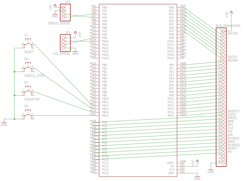
I went all out on the STM32 side, adding as much peripherals as possible, in the end I have SD card, I2C EEPROM, PS/2 Keyboard, RTC, ESP8266, and a general purpose UART header all hooked up to the STM32. It might be a bit overkill but I guess it’s better to have them just in case than not having them at all.
The STM32 will talk to the CPLD via a mini-bus with 4 bit of address, 8 bit of data, and a handful of control signals. While the CPLD contains all the glue logic to interact with the Z80 bus. Below is the diagram of the I/O board structure.
To program the CPLD I bought a cheap chinese knockoff programmer which seems work well enough, also needed is Altera Quartus Prime Lite, which is free. I’m going to use schematic capture for this instead of connecting everything in Verilog because I feel that being able to see and edit a schematic is more intuitive in this case. But first I need to write a couple of components that I’m going to use inside CPLD, chief among which is the 74HC573 8-bit transparent latch, a simple matter of 30 lines of code:
| module dlatch8( | |
| input wire [7:0] data, | |
| input wire LE_H, | |
| input wire OE_L, | |
| output reg [7:0] q | |
| ); | |
| reg [7:0] q_internal; | |
| // activates when LE_H or OE_L changes | |
| always @ (LE_H or OE_L) | |
| // output active, load inactive | |
| if (OE_L == 0 && LE_H == 0) begin | |
| // save the data to internal latch | |
| q <= q_internal; | |
| end | |
| // output active, load active | |
| else if (OE_L == 0 && LE_H == 1) begin | |
| // save the data to internal latch, and mirror it on the output | |
| q_internal <= data; | |
| q <= q_internal; | |
| end | |
| // output and load both inactive | |
| else if (OE_L == 1 && LE_H == 0) begin | |
| // do nothing, output high impedance | |
| q <= 8'bzzzzzzzz; | |
| end | |
| // output inactive, load active | |
| else begin | |
| // load internal latch while output high impedance | |
| q <= 8'bzzzzzzzz; | |
| q_internal <= data; | |
| end | |
| endmodule |
Another one we’re going to use is a 4-to-16 line decoder:
| module decoder_4to16 ( | |
| input enable, | |
| input [3:0] binary_in, | |
| output reg [15:0] decoder_out | |
| ); | |
| always @ (enable or binary_in) | |
| begin | |
| if (enable) begin | |
| case (binary_in) | |
| 4'h0 : decoder_out = 16'h0001; | |
| 4'h1 : decoder_out = 16'h0002; | |
| 4'h2 : decoder_out = 16'h0004; | |
| 4'h3 : decoder_out = 16'h0008; | |
| 4'h4 : decoder_out = 16'h0010; | |
| 4'h5 : decoder_out = 16'h0020; | |
| 4'h6 : decoder_out = 16'h0040; | |
| 4'h7 : decoder_out = 16'h0080; | |
| 4'h8 : decoder_out = 16'h0100; | |
| 4'h9 : decoder_out = 16'h0200; | |
| 4'hA : decoder_out = 16'h0400; | |
| 4'hB : decoder_out = 16'h0800; | |
| 4'hC : decoder_out = 16'h1000; | |
| 4'hD : decoder_out = 16'h2000; | |
| 4'hE : decoder_out = 16'h4000; | |
| 4'hF : decoder_out = 16'h8000; | |
| default : decoder_out = 0; | |
| endcase | |
| end | |
| else begin | |
| decoder_out = 0; | |
| end | |
| end | |
| endmodule |
And with that, we can start laying out our glue logic inside the CPLD. Instead laying down physical 74 chips, we can just do it in software and watch the magic happen. This I/O board needs to handle interrupts, port write, and port read. So let’s start with the first one:
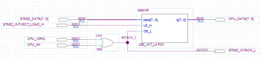
While it might look complicated at first, this is actually not that bad. The centrepiece is just a 8-bit latch. When the STM32 controller wants to start a Z80 interrupt, it first puts the interrupt vector on the STM32-CPLD data bus, then activates INTVECT_LOAD signal, this loads the vector into the latch. Then STM32 pulls down the INT line on the Z80 to start the interrupt, the Z80 will acknowledge the interrupt at the beginning of the next instruction, where both IORQ and M1 goes low. They are OR’ed together to give INTACK, which then activates the output enable of the latch, putting stored interrupt vector onto the CPU bus, which Z80 then combines with I register and jumps to that interrupt vector address. The INTACK also generates an interrupt on the STM32, upon which deactivates the INT line. Here is the STM32’s code snippet:
| void interrupt_activate(uint8_t vector) | |
| { | |
| // put the interrupt vector on STM32-CPLD bus | |
| CPLD_DATA_PORT->ODR &= 0xff00; | |
| CPLD_DATA_PORT->ODR |= vector; | |
| // load the interrupt vector latch inside CPLD | |
| data_output(); | |
| vect_load_activate(); | |
| vect_load_deactivate(); | |
| data_input(); | |
| // start the Z80 interrupt | |
| HAL_GPIO_WritePin(Z80_INT_GPIO_Port, Z80_INT_Pin, GPIO_PIN_RESET); | |
| } | |
| // ...meanwhile in STM32 pin change ISR | |
| void HAL_GPIO_EXTI_Callback(uint16_t GPIO_Pin) | |
| { | |
| // INTACK interrupt | |
| if(GPIO_Pin == INTACK_Pin) | |
| HAL_GPIO_WritePin(Z80_INT_GPIO_Port, Z80_INT_Pin, GPIO_PIN_SET); // turn off Z80 interrupt | |
| } |
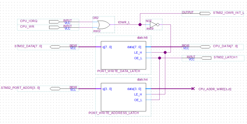
With that out of the way, next up is port write. It uses 2 transparent latches and it’s actually extremely similar as the interrupt above, only the data is loaded from Z80 side. When Z80 wants to write to a port, both IORW and WR goes low, which is OR’ed to give IOWR signal. When IOWR is low, there is valid port address and data on the CPU bus, so I made IOWR simply load the address and data into the corresponding latches. IOWR also fires an interrupt on the STM32, who will then activate the latch1 signal and read the data and address off the latches and process them. Below is the diagram and code snippet.
| // STM32 pin change interrupt handler | |
| void HAL_GPIO_EXTI_Callback(uint16_t GPIO_Pin) | |
| { | |
| // IOWR interrupt | |
| if(GPIO_Pin == IOWR_Pin) | |
| { | |
| // switch to input | |
| data_input(); | |
| addr_input(); | |
| // enable address and data latch outputs | |
| latch1_activate(); | |
| // process port address and data | |
| vport_raw = CPLD_DATA_PORT->IDR; | |
| vport_addr = (uint8_t)((vport_raw & 0xf00) >> 8); | |
| vport_data = (uint8_t)(vport_raw & 0xff); | |
| latch1_deactivate(); | |
| } | |
| } |
Next up is port read, this is the most complex of the three because of the timing constraints. Let’s look back at port write first: when CPU does a port write, the port address and data are loaded into two transparent latches, while STM32 is notified at the same time. So even if STM32 bogged down for some reason the port address and data will still be available in the latch, nothing is lost.
There is no such luxury in the case of port read, when Z80 wants to read a port, both IORQ and RD goes down, OR’ed together to give IORD. Port data must be valid the moment IORD goes active, otherwise the CPU gets garbage data. That means I can’t make STM32 respond to IORD as an interrupt since it would already be too late. So as you probably have guessed, transparent latches to the rescue again.
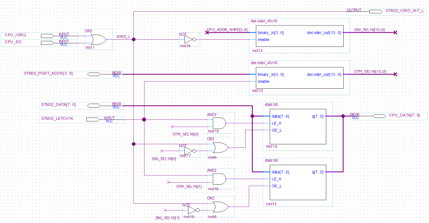
This is much more complicated than the first two so bear with me: There are 16 transparent latches, corresponding to 16 available Z80 ports. When Z80 wants to read one of these ports, a valid port address will be present on the CPU bus, then the IORD signal goes active. When that happens a 4-to-16 decoder is activated and selects the corresponding latch out of the 16 based on the address on the CPU bus, this select signal along with IORD itself enables the output of that latch, putting its content onto the data bus instantly.
Of course we need be able to write data into those latches first for CPU to read. When STM32 wants to load data into a latch, it puts the address and data onto the STM32-CPLD bus, then activates the LATCH16 signal. This enables another 4-to-16 decoder inside CPLD that select the corresponding latch. The select signal together with LATCH16 signal loads the data into said latch, which will then be available for CPU to read. The STM32 code is actually pretty simple:
| // loads a port for CPU to read | |
| void load16(uint8_t address, uint8_t data) | |
| { | |
| // put the address and data onto STM32-CPLD bus | |
| uint16_t value = 0; | |
| value = (address & 0xf) << 8; | |
| value = value | data; | |
| CPLD_DATA_PORT->ODR &= 0xf000; | |
| CPLD_DATA_PORT->ODR |= value; | |
| data_output(); | |
| addr_output(); | |
| // load the latch | |
| latch16_activate(); | |
| latch16_deactivate(); | |
| data_input(); | |
| addr_input(); | |
| } |
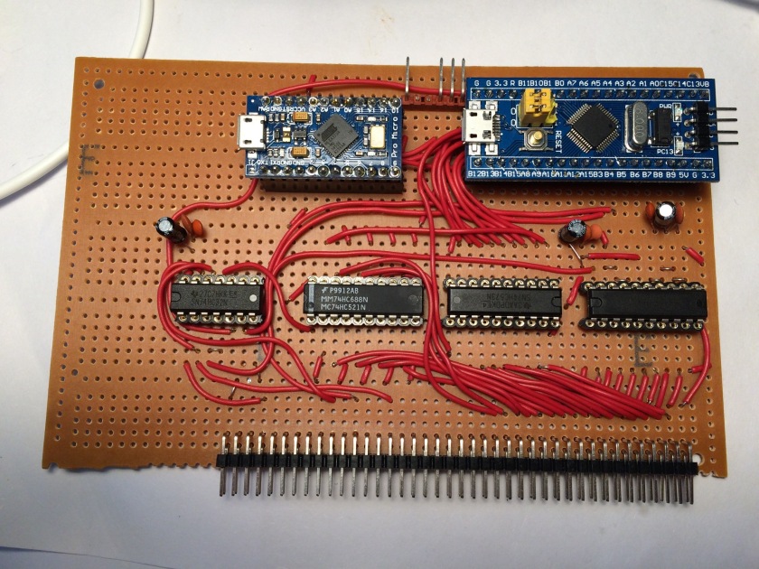
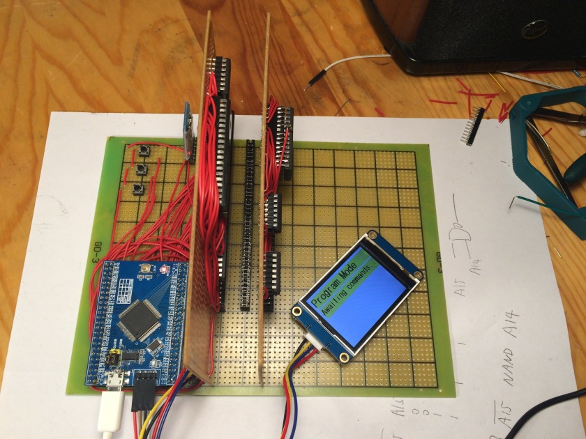
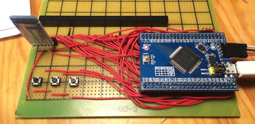
With all those out of the way, here is the finished board:
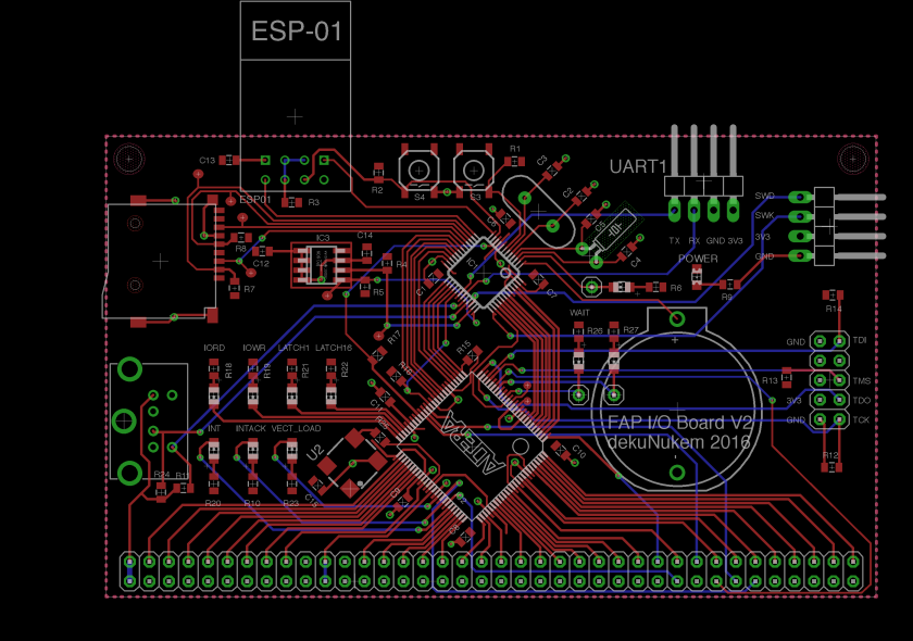
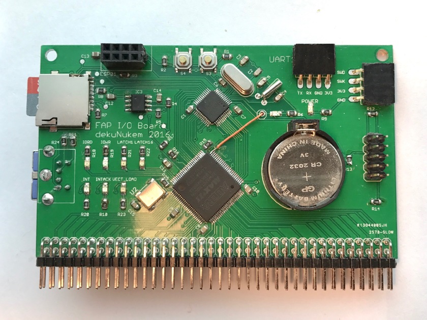
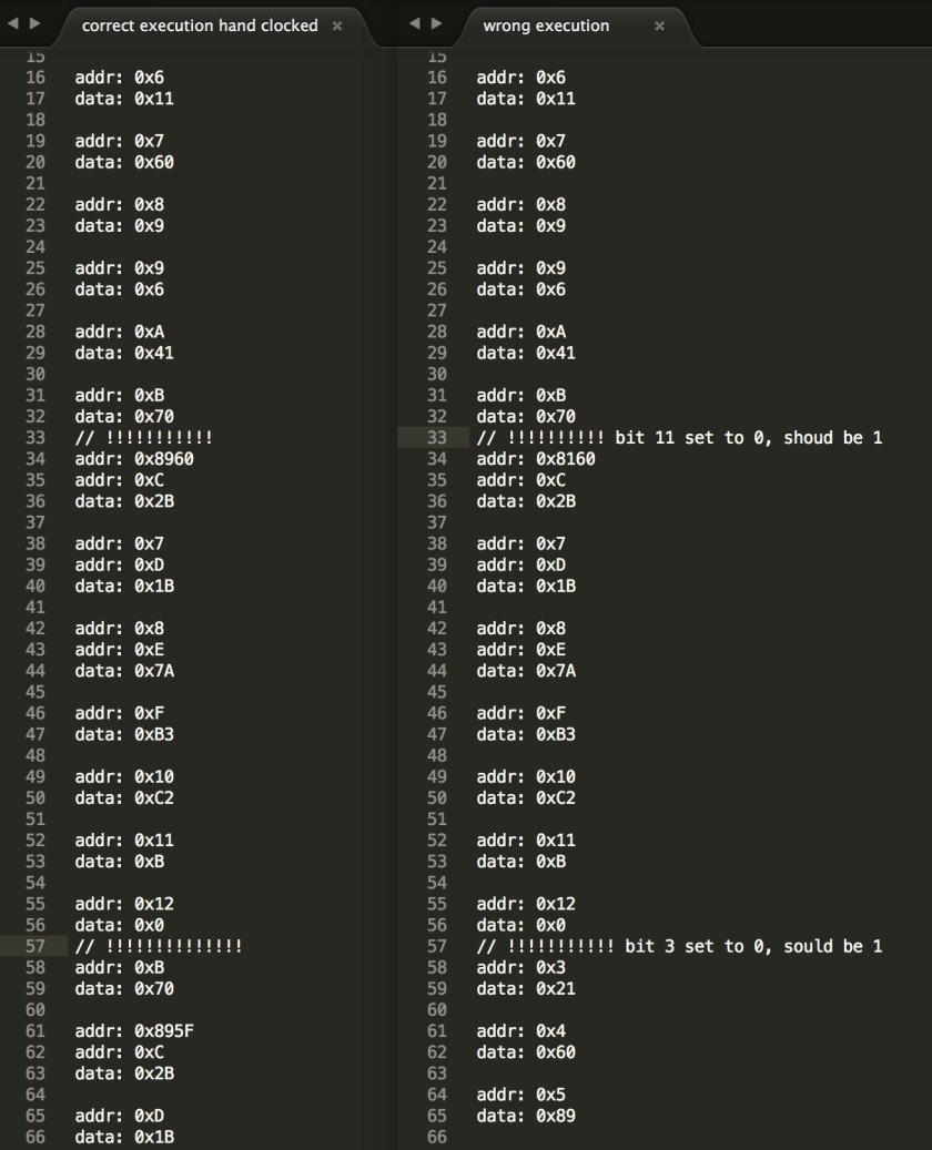
Again, I made some mistakes in the rush to get the board made, the footprint of PS/2 connector is flipped, the JTAG connector pinout is all wrong, and somehow I missed the TDO line. Those are all fixed in the repo. And with just one jumper wire, the board functions perfectly.
Previous article: CPU board, memory board, video card.