Previous Post: VGA Character Generator
Next Post: FAP says Hello World
In my last post I designed and built an early stage of FAP’s video card on breadboard, I decided to use VGA for video output, running 80×30 text mode at 640×480. The VRAM was working, so was the character ROM, and now the board is rendering garbage data in VRAM on start up as characters on screen, all is good.

However, there was still some glaring issues left untouched in the last post, for example the lack of colors. That would be the job of the attribute byte. In my design(and a lot of other early PCs) each text mode character is accompanied by an attribute, which describes what color is the said character, should it be blinking, etc. I ignored it last time to get the character generator working faster, now since it does, it’s time to go back to that.
First a little bit about the VRAM layout, the 80×30 text mode needs 2400 bytes for character, and another 2400 for attribute. Those 4800 bytes will be mapped to between 0x8000 and 0x92c0 in Z80’s memory, first 2400 for char and second half for attribute.
Here is updated verilog file with attribute fetching:
| always @(posedge clk50) | |
| begin | |
| // inside active region | |
| if ((vc >= vbp && vc < vfp) && (hc >= hbp && hc < hfp)) | |
| begin | |
| front_vram_rd_low = 0; | |
| hpos = hc - hbp; | |
| vpos = vc - vbp; | |
| hdot = hpos[2:0]; | |
| vdot = vpos[3:0]; | |
| hchar = hpos[9:3]; | |
| vchar = vpos[9:4]; | |
| if (fetch_attribute) begin | |
| front_vram_addr = 80 * vchar + hchar; | |
| attribute_data = front_vram_data; | |
| end | |
| else begin | |
| front_vram_addr = 80 * vchar + hchar + 2400; | |
| char_data = front_vram_data; | |
| end | |
| fetch_attribute = ~fetch_attribute; | |
| red = font_pixel ? attribute_data[5:4] : 0; | |
| green = font_pixel ? attribute_data[3:2] : 0; | |
| blue = font_pixel ? attribute_data[1:0] : 0; | |
| end | |
| // outside active region | |
| else | |
| begin | |
| fetch_attribute = 1; | |
| front_vram_rd_low = 1; | |
| front_vram_addr = 13'bzzzzzzzzzzzz; | |
| red = 0; | |
| green = 0; | |
| blue = 0; | |
| end | |
| end |
This block is now being clocked by the 50MHz internal clock, and the fetch_attribute alternates between 0 and 1 at each clock cycle. At the clock cycle where fetch_attribute is 0 the FPGA gives the character address to the VRAM, and when fetch_attribute is 1 the attribute address. Then the character is looked up in character ROM, while lower 6 bits of attribute is sent to DAC directly, giving colors. Here is what it looks like:

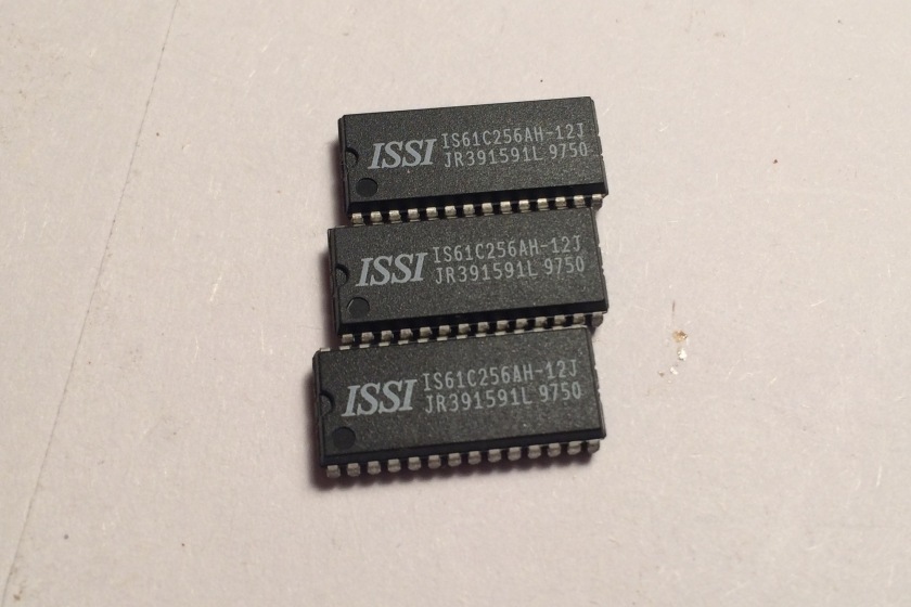
However, the fuzziness is back again. I can think of several reasons: the VRAM is now being accessed twice for every pixel, once for character once for attribute. This could mean it might be too slow again. The pixel clock is 25MHz, which means each clock cycle is 40ns, two memory access during this period means each access only has 20ns, and my VRAM is rated 15ns, so it’s very close. The faster speed also generates more noise, especially on the breadboard. Lastly, the monitor’s auto optimization seems a bit off on the signal of my video card. I bought some 12ns IS61C256 chips, it’s only 3 ns faster, but in FAP, every nanosecond counts.
I put it on, and it looks a little bit better, but not by much, since there is still the noisy breadboard. I’ll have to wait until I build the thing on the stripboard.
Now that the video card is mostly working by itself, we come to the issue of how to interface it with the CPU. As you know the VRAM holds the characters and attributes that will be rendered on screen, however that requires CPU writing something into it in the first place, but the VRAM is being read by the video card most of the time so the only time that CPU have the chance of writing into it is one of the blanking periods, namely Horizontal Blanking Interval and Vertical Blanking Interval. HBLANK happens every scanline but its duration is extremely short, only around 6us if I remember correctly, our 1970s Z80 won’t have enough time to push a lot of useful things into VRAM during that kind of time, and even if it does it will probably cause screen tearing or visual artifacts, since it change the content of a single pixel line instead of an entire frame. So that leaves us with VBLANK, that lasts around 1.6ms every single frame, which is plenty of time, but that means CPU will have to spend 90% of its time doing nothing but waiting for VBLANK, which is extremely wasteful, that is what Quinn chose to do with her Veronica. One way to get around this is to use a Dual Port RAM which allows write and read at the same time, but that stuff is pretty hard to find. I decided to use my existing parts and implement the tried-and-true method of freeing CPU from waiting for the beam: Double Buffering.
The principle of double buffering is actually pretty simple: two VRAMs, called back and front VRAM, are used. The CPU writes to back VRAM, and during the VBLANK period the content of back VRAM is copied to the front VRAM and subsequently rendered. This way CPU can write to VRAM at anytime it wants, apart from a miniscule amount of time during copying. Screen tearing and artifacts are also eliminated since the entire frame is being modified. The only possible downsides are probably cost and complexity, but I think it would be worth it in the end, when I won’t need to race the beam while writing my programs.
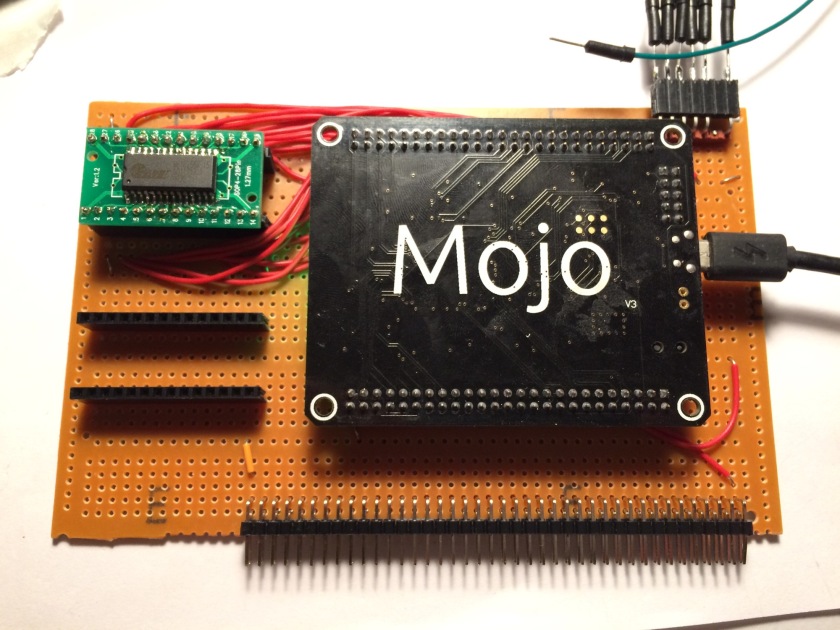
However, at this stage the noise problem on the breadboard is pretty obvious now, and adding another VRAM and 28 wires will only make it worse, so I decided to just build it on the board.
And to make sure I don’t make wiring mistakes I decided to start again and retest everything from the beginning again, firstly just the FPGA and DAC, displaying color bars.

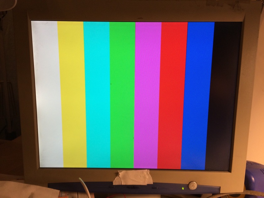
Good, that works. Next step is hooking up one VRAM and try rendering the garbage data again.

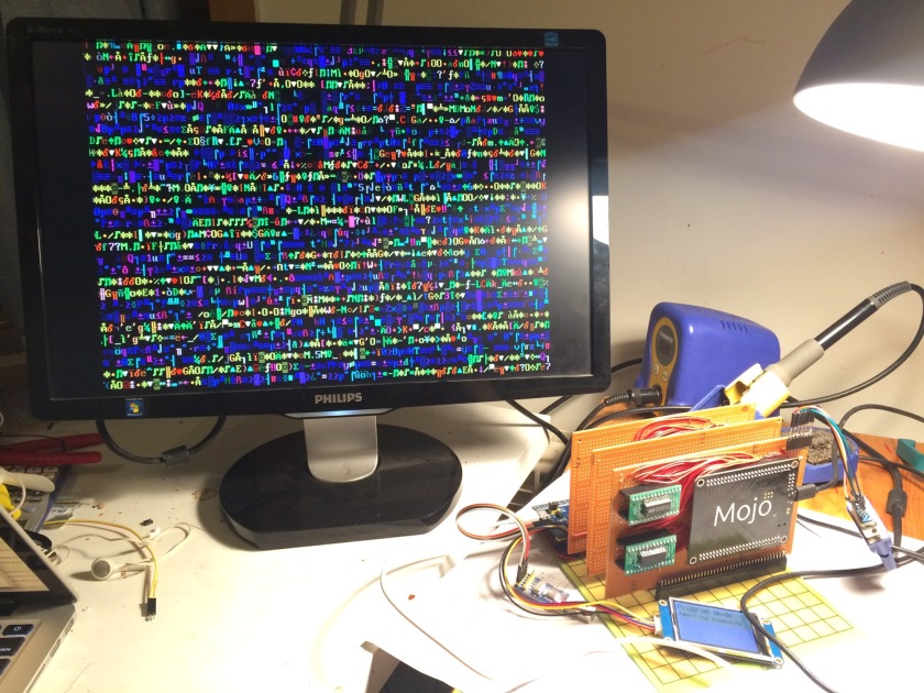
Notice how all the noises are gone, good stuff, a lot of U’s for some reason.
Coming up next is the main course of this post: double buffering.
| module buffer_copier( | |
| input wire clk, | |
| input wire vblank, | |
| output reg front_vram_wr_low, | |
| output reg back_vram_rd_low, | |
| output reg copy_in_progress, | |
| inout wire [7:0] front_vram_data, | |
| inout wire [7:0] back_vram_data, | |
| output wire [12:0] front_vram_addr, | |
| output wire [12:0] back_vram_addr | |
| ); | |
| reg [12:0] counter; | |
| assign front_vram_data = copy_in_progress ? back_vram_data : 8'bzzzzzzzz; | |
| always @(posedge clk) | |
| begin | |
| if (vblank == 0) begin | |
| back_vram_rd_low <= 1; | |
| front_vram_wr_low <= 1; | |
| copy_in_progress <= 0; | |
| counter <= 0; | |
| end | |
| else if (counter <= 4800) begin | |
| back_vram_rd_low <= 0; | |
| front_vram_wr_low <= 0; | |
| copy_in_progress <= 1; | |
| counter <= counter + 1; | |
| end | |
| else begin | |
| copy_in_progress <= 0; | |
| back_vram_rd_low <= 1; | |
| front_vram_wr_low <= 1; | |
| counter <= 0; | |
| end | |
| end | |
| assign back_vram_addr = copy_in_progress ? counter : 13'bzzzzzzzzzzzzz; | |
| assign front_vram_addr = copy_in_progress ? counter : 13'bzzzzzzzzzzzzz; | |
| endmodule |
The module waits for the vblank interval, and when it arrives it enables the read of back VRAM and write of the front VRAM, then starts a counter that goes to 4800, which doubles as the address for both front and back VRAM. This way the content of back VRAM is copied to the front as counter increments. The copy_in_progress signal is made available so that other modules as well as the CPU can know if a buffer copy is under way. The total copy time is around 192us, this means instead of having to wait 90% of the time to write to the VRAM, the CPU now only have to wait 1.1% of the time instead. A pretty big improvement.
I added another slot on FAP’s backplane and plugged the video card in, it’s practically indistinguishable from a GTX980 to be honest.
Until now the video card has been working by itself, copying buffers and rendering characters. However sooner or later CPU will have to be able to control it. There are some ways that CPU can talk to the GPU, certain computers map their VRAM directly to the addressable memory (NES and Gameboy comes to mind), while others chose to not expose the VRAM and instead have memory mapped GPU registers, MOS Technology 8568 and VIC-II belong to this kind. For FAP, I decided to use both. VRAM will be mapped to between 0x8000 and 0x92c0, while virtual registers somewhere after that. This way I can easily test something by writing directly into VRAM, while I can also ask GPU to do heavylifting operations like text scrolling, it’s the best of both words.
For now though, it’s just the write-only VRAM mapping, here is the code:
| module cpu_vreg( | |
| input wire clk, | |
| input wire copy_in_progress, | |
| input wire cpu_rd, | |
| input wire cpu_wr, | |
| input wire cpu_mreq, | |
| input wire [15:0] cpu_addr, | |
| inout wire [7:0] cpu_data, | |
| output reg back_vram_wr_low, | |
| output reg [12:0] back_vram_addr, | |
| output reg [7:0] back_vram_data | |
| ); | |
| always @(posedge clk) | |
| begin | |
| if(copy_in_progress == 0 && cpu_wr == 0 && cpu_mreq == 0 && cpu_addr >= 16'h8000) begin | |
| back_vram_addr = cpu_addr[12:0]; | |
| back_vram_data = cpu_data; | |
| back_vram_wr_low = 0; | |
| end | |
| else begin | |
| back_vram_wr_low = 1; | |
| back_vram_addr = 13'bzzzzzzzzzzzzz; | |
| back_vram_data = 8'bzzzzzzzz; | |
| end | |
| end | |
| endmodule |
This simple module checks if the MREQ and WR is low and address is in the correct range, and connects the CPU bus to back VRAM if it does. I’ll implement VRAM read and virtual registers later, I can already print some pretty text with just write for now.
Time to write a Z80 program to try it out, if I start to write a value from the back of the VRAM to front, the screen should first change color, since addribute bytes are at the back of the VRAM, once attribute bytes have been filled, text will start appearing as the value fills up the character portion of the VRAM. Here is the test program:
| org 0x0 | |
| start: xor d | |
| xor e | |
| xor b ; clear d, e, b | |
| ld hl, 0x92c0 ; load hl with address of back of the VRAM | |
| ld de, 2400 ; 2400 bytes of attributes | |
| ld b, 0x1b ; color, 0x1b is 011011, should be purple | |
| attri: ld (hl), b ; store the color into VRAM address at hl | |
| dec hl ; decrease hl to move on to next VRAM address | |
| dec de ; decrease the counter | |
| ld a,d | |
| or e ; check if counter is 0 | |
| jp nz,attri ; continue looping if it's not | |
| ld de, 2400 ; now attributes have been filled, reload the counter | |
| ld b, 65 ; ASCII code for letter A | |
| char: ld (hl), b ; similarly loop as above, fill the chatacter VRAM | |
| dec hl | |
| dec de | |
| ld a,d | |
| or e | |
| jp nz,char | |
| end: jp end ; all done |
The program first fills the bottom half of the VRAM with 0x1b, binary 011011, the first 01 goes to red DAC, middle 10 goes to green DAC, and last two bit 11 goes to blue DAC, the result should be a violet color. After filling up attribute the program then fills the first 2400 bytes of VRAM with 65, ASCII of letter A. So we should expect the garbage text on screen first turn violet, then fill up with letter A. Here is what happens:
Well it’s mostly what should be happening, however, some characters didn’t turn violet, and there are few missed A’s here and there. This was because CPU was trying to write during the VRAM copy operation and was ignored. My next step would be implementing a few virtual registers so CPU can check if GPU is busy before trying to write to VRAM. But anyhow, progress is progress.
There was actually a extremely frustrating backstory that I didn’t mention, after trying to get the above code work at around 500Hz, I tried to bump up the processor speed to around 500KHz and it simply would not work. Sometimes it enters the end loop early, sometimes it ignores the loop entirely and continues past the end of the program. I thought there was a loose connection or weak short somewhere along the bus but after inspecting and cleaning the board the problem still happens from time to time. I eventually let my STM32 controller print out the address and data content after each clock cycle, here is one of the executing traces:
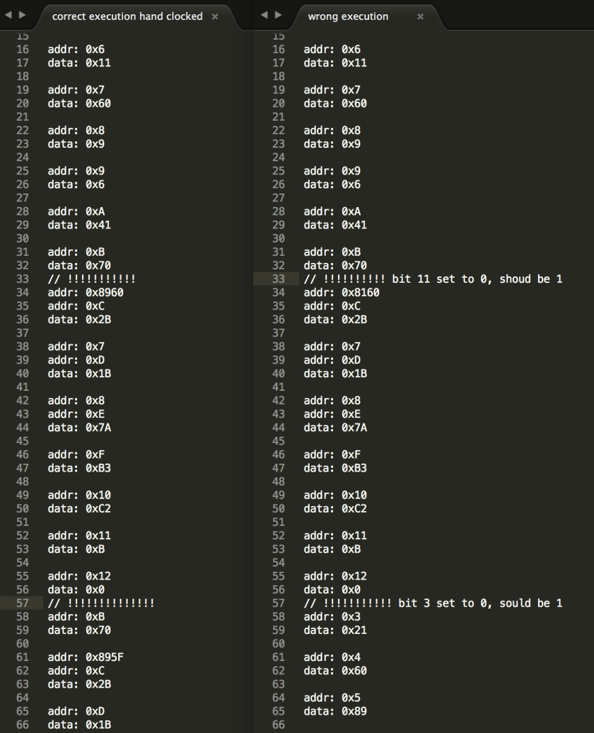
As you can see address bus is missing bits, 0x8960 turned into 0x8160, and jumping to 0xb turned into jumping to 0x3, that’s why my program was going all over the place. The culprit? Noise. After adding a couple of caps bewteen VCC and GND of the Z80 and memory chip, the problem went away. However I did spent a stupidly long amount of time trying to nail it down. It’s one of the things I should have known better, oh well.
Anyway, FAP’s video card is halfway working now. I’ll finish up the GPU virtual register in the next post, and have my FAP finally say “hello world” like all the great computer did when they were born.

Wow Deku OneHand
LikeLike
Erm, did you read the spec sheet for the Spartan 6 FPGA in the Mojo? There are 576kbits of dual ported BRAM on board. You could implement the character ROM, screen and attribute RAM inside of the FPGA.
The second point is that you should pipeline your data. Don’t try to do all processes inside of one clock. The final DAC step should be doing little more than shifting bits out of a register. Earlier parts of the pipeline should fetch the character and attribute, look up the character data etc. Your original 150nS ROM should have been quite fast enough with a properly pipelined process.
LikeLike